 130xe to 576kxe
The 130XE/576K upgrade, by Scott Peterson.
Copyright (C) 1986, released to the public.
Here we go again, this time I recommend you have some electronics experience
if you wish to preform the upgrade. Some of the work is duplicated from the
320K upgrade so 320XE owners will not have as much work to do. One other
point, when in the 576K mode you MUST use some sort of basic cart. as you lose
the internal basic, this is only in the 576K mode, in the 130XE mode internal
basic will function normally.
TOOLS NEEDED;
To perform this upgrade you need the following;
Low wattage fine tip soldering iron.
Vacuum de-soldering tool (like Radio Shack PN#64-2098).
Some 30-gauge wire (Radio Shack PN#278-501).
#2 Phillips head screwdriver.
Heat-shrink tubing, 1/8 in. Dia.
Also a pair of small needle-nose pliers and a small flat tip screwdriver are
handy.
PARTS NEEDED;
Z1 74LS158
Z2-Z17 41256(150ns.)
Z18 74LS138
Z19 7432
R1-R2 33 ohm 1/4 watt resistor.
S1 Micro-mini DPDT switch(like Radio Shack PN#275-626)
Remove the 130XE case and metal RF shield to get down to the mother
board.(320XE users go to step two).
STEP ONE:
Now de-solder and remove the eight ram chips U26 thru U33(MT4264). They are
the row closest to the TV RF module (do NOT use solder wick, the circuit board
of the 130XE has very weak runs and they will pull loose if not completely
de-soldered). Replace these with the 16 pin low profile sockets. Take a piece
of wire approx 12 in. long and run a jumper from pin 1 of each socket to the
next. When you are done the wire should be attached to pin 1 of each of the
new sockets and you should have about 6 inchs left over. Do this on the rear
of the mother board and then snake the wire thru the large hole near the ram
chips.
Next, desolder and remove U23(CO14795), and replace it with a 40 pin socket.
Bend up pins 15 and 16 and insert it in the socket you just installed. Take
Z1(74LS158) and break off pins 5,6,7,9,10,11,12,13,14. Bend up the other
pins on it except 8 and 16. Put this "piggy back" on top of
U20(HD14050, or 4050 - located just to the right of C50) and solder pins 8 and
16 of Z1 to pins 8 and 16 on U20. Now take a short jumper from pin 15 on Z1 to
pin 8 of Z1. Take a piece of wire about 4 in. long, solder one end to pin 30
on the chip marked "CO14805" on the mother board, and the other end
to pin 1 on Z1. Next solder a wire to pin 15(one of the two you bent out) of
U23 and connect the other end to pin 2 on Z1. Solder a wire to pin 16 on U23
and connect the other end to pin 3 on Z1.
Take R1(33 ohm) and trim the leads to about 1/4 in. Take the wire you
connected to pin 1 of the ram chip sockets and solder it to one end of R1,
solder the other end of R1 to pin 4 on Z1.
STEP TWO:
Slide the mother board back into the bottom half of the plastic case (do not
use the RF shield, you must be able to get at the mother board), and attach
the keyboard. It will rest above the mother board without touching it. Test
all 41256 ram chips by putting one set of 8 in the sockets and using the
handlers (or DOS's), and then the next. After testing all ram chips remove
them all from the sockets, and take 8 of them and cut about half of pin 15 off
of each one. Only the "fat" part of pin 15 should be left. After
doing this you have to "piggy back" the 8 256K ram chips with the
short pin 15's on top of the other 8 256K ram chips. Now solder all the pins
together on the stacked ram chips except for pin 15, it should not be touching
the other pin 15, make sure you have them going pin 1 to 1, pin 2 to 2,ect.
When you get done you will have 8 sets of Piggy backed 256K ram chips. Now
take a piece of wire about 16 in. long and run a jumper from pin 15 to the
next one on all the top 256k DRAM's, leaving about 1 inch between each ram
chip. Put these stacked ram chips into the 8 sockets you installed earlier.
Take Z18 (74LS138) and bend up all the pins except 8 and 16, cut the pins you
bent up in half so only the fat part is left, and solder pins 8 and 16 to
pins 8 and 16 of the other 74LS138 right below the U23(CO14795). Take Z19 and
bend up all pins except 7 and 14, once again cut all the pins you bent up in
half and solder pins 7 and 14 to pins 7 and 14 of the 74LS08 right
below U23.
Take the wire you jumpered earlier to pin 15 of Z10 thru Z17(the upper row of
256K ram chips) and go out 2 in. and cut the wire, now install R2(33 ohm)
between this cut. Place a piece of heat shrink tubing over R1 and make sure no
wire is exposed and heat it with a lighter. Take the other end of this wire
and connect it to Z18 pin 14. Find the 2 33 ohm resistors just to the right of
U28(one of the ram chips you socketized). The upper one of the 2
is R111, desolder the right leg of it and bend it up. Take a piece of wire and
solder it to the land where you just removed the leg of R111. Connect the
other end to Z18 pin 4. Trim back the leg of R111 and solder a wire to it,
slip a piece of heat shrink tube over it and heat it up. Now connect the other
end to Z18 pin 12. Take a short wire and run a jumper from pins 1 and 16 of
Z18. Take another short wire and connect a jumper from pins 3,5, and 8 of Z18.
Now connect a wire from Z18 pin 2 to Z19 pin 3. Find the wire you installed
from U23 pin 15 to Z1(74LS158) pin 2 and desolder it from U23. Take it and
reconnect it to Z19 pin 11. Ok, now pry U23(CO14795) back out of the socket
and bend up pin 11, plug it back in. Run a jumper from pins 1 and 4 of Z19,
and another jumper from pins 10 and 13 of Z19. Connect a wire from U23 pin 11
to Z19 pin 1, and from U23 pin 15 to Z19 pin 13. Now connect a wire from Z19
pin 8 to the right side of the 3.3K ohm resistor marked R206 (located at the
bottem right of U23). Connect a wire to Z19 pin 6 and run it to pin 18 of
U3(CO61618). Now comes the tricky part, drill a small hole(1/4 in. or so,
depending on the switch size) at the rear right on the back of your 130XE.
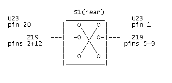
Take the small DPDT switch(S1) and install it in the hole. Now connect it as
shown (make sure the switch DOESNT have a center off position);

Note: where the wires cross in the middle, they are NOT connected. Make the
connection from the switch to U23 on the rear of the mother board. Well that's
it (thank god). Now re-assemble the computer, being careful not to break any
wiring going to the switch. You should now have in one switch position a 100%
compatible 130xe, and in the other you have a 576K 130XE that does not have
Antic memory enhance mode and also can-not use internal basic. In the 130XE
mode you gain 64K as bit 6 of the PIA can still be used. The following page
list of the bit table and numbers to be used in location 54017(PORTB). Once
again, if you need help call the Peanut Gallery BBS (408)-384-3906. If you
want a mailer of all the upgrades I have as well as a disk with handlers,
source codes, ect.
send a money order (please, no checks) for $10.00 to;
Scott Peterson
P.O.Box 33
Ft.Ord CA. 93941-0033
This includes the 800 288K upgrade by D.G.Byrd, the 800XL/256K(C.Burchholz),
the 130XE/320k upgrade and anything else I finish. Good luck, and have fun.
Memory Control Register 54017(D301)
130XE in 576K mode.
Bit 7 6 5 4 3 2 1 0
D a b C c d e R
D=0 enable diag. ROM
R=1 enable OS ROM
C=0 enable extended memory
abcde= memory control bits.
-------------------------------------
Bank# Control#(dec) Hex
-------------------------------------
Bank 0 ---------->129 81
Bank 1 ---------->131 83
Bank 2 ---------->133 85
Bank 3 ---------->135 87
Bank 4 ---------->137 89
Bank 5 ---------->139 8B
Bank 6 ---------->141 8D
Bank 7 ---------->143 8F
Bank 8 ---------->161 A1
Bank 9 ---------->163 A3
Bank 10 --------->165 A5
Bank 11 --------->167 A7
Bank 12 --------->169 A9
Bank 13 --------->171 AB
Bank 14 --------->173 AD
Bank 15 --------->175 AF
Bank 16 --------->193 C1
Bank 17 --------->195 C3
Bank 18 --------->197 C5
Bank 19 --------->199 C7
Bank 20 --------->201 C9
Bank 21 --------->203 CB
Bank 22 --------->205 CD
Bank 23 --------->207 CF
Bank 24 --------->225 E1
Bank 25 --------->227 E3
Bank 26 --------->229 E5
Bank 27 --------->231 E7
Bank 28 --------->233 E9
Bank 29 --------->235 EB
Bank 30 --------->237 ED
Bank 31 --------->239 EF
-------------------------------------
There is a version of MYDOS to support this mod, its called 4.1A and will run
up to 32 16K banks. At this time ICD is working on a RD.COM file to support
this. Also I have written a machine lang. tester that will load and test all
32 banks of memory to insure that they are there and work.
Good luck
Scott Peterson
There is a Ramdisk.com file in the D/load section of this WEB to support this
upgrade. It work's very well, as I am using a 576k 130XE on this BBS.